Problem Description:
Voltage, Current and Power analysis is very essential for the PCB. On a high power supply system it is very important to understand how the traces are behaving when a specific current or Voltage is driven across the PCB. Understanding what are the hotspots on the PCB which can lead to the PCB failures is one of the biggest challenges.
Business Challenges:
The principal challenge is to distribute the power across the PCB with a minimal Voltage drop over a longer length of the Traces so that the efficiency of the system can be improved. The exercise calls for a proper design of a PCB layout that would reduce the hot spots on the PCB prior to manufacturing. Consequently, via currents on the PCB can be Monitored and edited to do what if analysis before the PCB is given for Fabrication.
Technology Used:
ANSYS SiWave DC
Engineering Solution:
The Physics of the problem permits representation of the PCB as 2.5D axisymmetric. ANSYS SiWave 2.5D was used to perform DCIR analysis to simulate the Voltage and current distribution in the domain of analysis. Analyses of the PCB with Current, Voltage, Power at different traces and planes has enabled predict the DC Analysis of the PCB
Methodology Adopted:
- The ANSYS pioneered Automatic Adaptive Mesh Generation Algorithm divides copper traces into smaller elements to consistently arrive at suitable Mesh counts.
- For a typical AC-DC convertor with a output of 900W is performed
- The Ports are created between the input and output of the PCB by identifying the Critical hotspots for Analysis
- The voltage sources and current sinks are assigned to different ports on the PCB
- An initial analysis of Current density is carried out followed by the voltage and Power plane analysis.

Figure 1 - Current Density
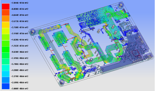
Figure 2 - Current Density
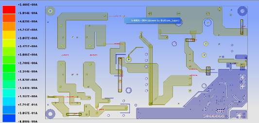
Figure 3 - Via Current
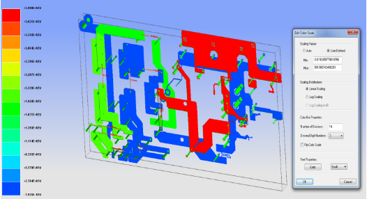
Figure 4 - Voltage distribution
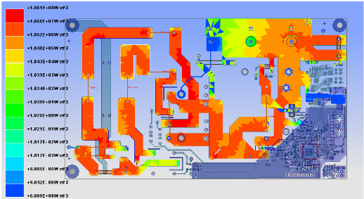
Figure 5 - Power Density
Entuple’s Team :
Entuple has a team of field application engineers and senior industry experts who can train the students on concepts of VLSI design. VLSI training provided by Entuple is focused on making students industry ready. We are proud to be one of the most in-depth training providers across India.
Benefits:
- Performing DCIR Analysis of the PCB helps us visualize, determine the PCB hotspots prior to the manufacturing of the PCB and helps to modify and do what if analysis of the PCB trace widths and via sizes so that the requirement is met as desired during the final manufacturing of the PCB. Performing this analysis can help us also understand what are going to be the estimated losses across the traces and planes of the PCB.
More over the current and power density simulation data greatly aids the combined Multiphysics-based board-level electro-thermal co-simulation provided by a link between the SiWave electromagnetic field solver and the ANSYS Icepak thermal analysis solver for electronics packages